
link:https://pan.baidu.com/s/1x1MJUyIPcyBShVWBxSUfMg Extraction code:jml6
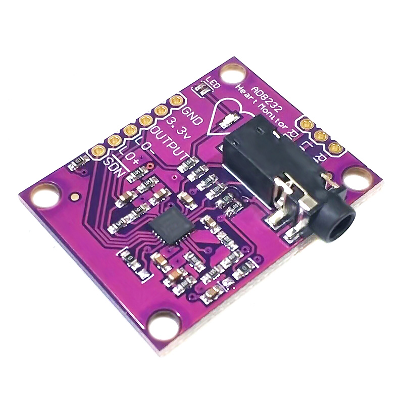
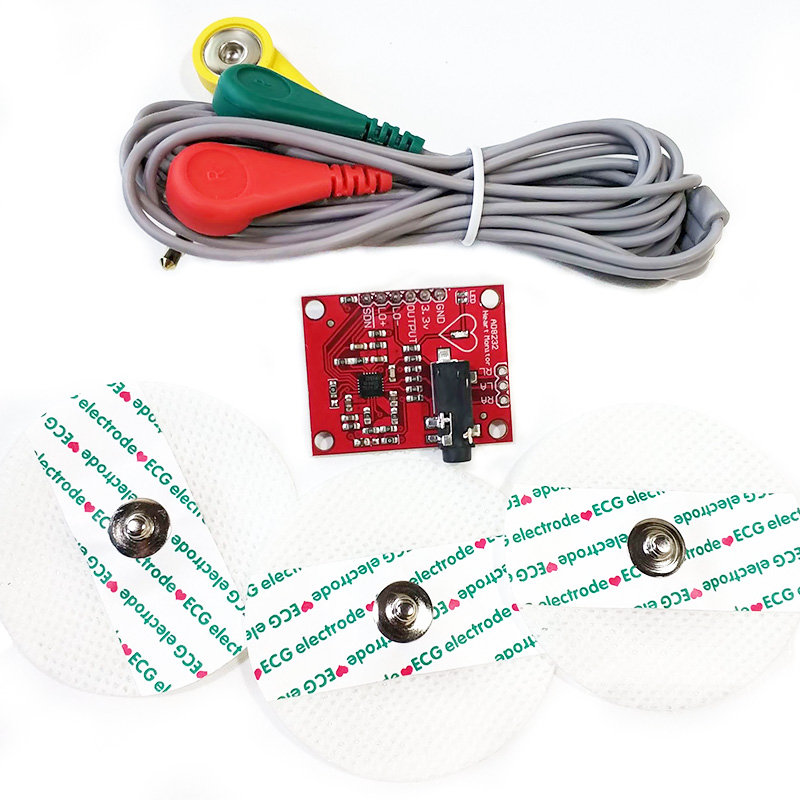
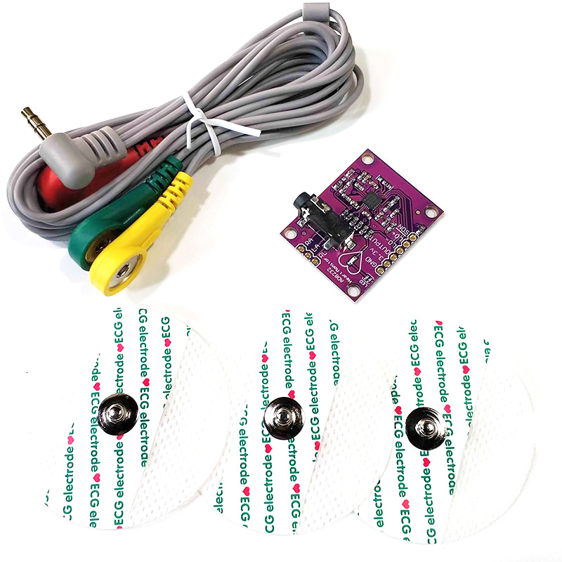
AD8232 sensor module
Single-lead heart rate monitoring front end
AD8232 is an integrated front end, suitable for signalling cardiac bioelectrical signals
No. conditioning for heart rate monitoring.
An integrated signal conditioning module for ECG and other bioelectric measurement applications. The device is designed to extract, amplify and filter weak bioelectric signals in the presence of noise caused by movement or remote electrode placement. This design enables an ultra-low power analog-to-digital converter (ADC) or embedded microcontroller to easily collect the output signal.
AD8232 uses a two-pole high-pass filter to eliminate motion artifacts and electrode half-cell potential. The filter is tightly coupled with the instrumentation amplifier structure, which can realize single-stage high-gain and high-pass filtering, thereby saving space and cost.
AD8232 uses an unused constrained operational amplifier to create a three-pole low-pass filter, eliminating additional noise. The user can select the cutoff frequency of all filters to meet the needs of different types of applications.
In order to improve the common-mode rejection performance of the system line frequency and other undesirable interference, AD8232 has a built-in amplifier for driven lead applications such as right-side drive (RLD).
The AD8232 includes a fast recovery function, which can reduce the long set-up tail of the high-pass filter. If there is a sudden change in the amplifier rail voltage (such as a lead-off situation), the AD8232 will automatically adjust to a higher filter cut-off state. This function allows the AD8232 to achieve rapid recovery, so that a valid measurement value can be obtained as soon as possible after the lead is connected to the electrode of the measurement object.
The rated temperature range for guaranteed performance is 0 ℃ to 70 ℃, and the operating temperature range is -40 ℃ to +85 ℃.
application
Fitness and exercise heart rate monitoring
Portable ECG
Remote health monitoring
Gaming peripherals
Bioelectric signal acquisition
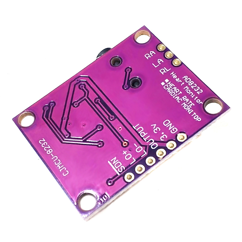
Pin number Pin name Description
1 HPDRIVE high-pass driver output. HPDRIVE should be connected to the capacitor in the first high-pass filter.
AD8232 drives this pin to keep HPSENSE at the same level as the reference voltage.
2 +IN The positive input terminal of the instrumentation amplifier. +IN is usually connected to the left arm (LA) electrode.
3 −IN The negative input terminal of the instrumentation amplifier. −IN is usually connected to the right arm (RA) electrode.
4 RLDFB Right leg drive feedback input terminal. RLDFB is the feedback pin of the right leg drive circuit.
5 RLD Right leg drive output terminal. The drive electrode (usually the right leg) should be connected to the RLD pin.
6 SW Fast recovery switch pin. This pin should be connected to the output of the second high-pass filter.
7 OPAMP+ Operational amplifier non-inverting input terminal.
8 REFOUT Reference voltage buffer output terminal. The instrumentation amplifier output is referenced to this potential.
REFOUT should be used as a virtual ground at any point in the circuit where a reference signal is needed.
9 OPAMP− The inverting input terminal of the operational amplifier.
10 OUT Operational amplifier output terminal. This output provides a fully conditioned heart rate signal.
OUT can be connected to the input terminal of the ADC.
11 LOD− The lead falls off the output of the comparator. In the DC lead-off detection mode, when the −IN electrode is disconnected,
LOD− is in a high level state, otherwise it is in a low level state. In the AC lead-off detection mode, LOD− is always in a low state.
The lead falls off the output of the comparator. In the DC lead-off detection mode, when the +IN electrode is disconnected, LOD+ is in a high level state,
Otherwise, it is in a low level state. In the AC lead-off detection mode, when the −IN or +IN electrode is disconnected, the LOD+ is at a high level.
When these two electrodes are connected, they are in a low level state.
12 LOD+
13 SDN Shutdown control input terminal. Drive SDN to a low level to enter a low-power shutdown mode.
14 AC/DC lead off mode control input terminal. For the DC lead-off mode, the AC/DC pin should be driven to a low level.
For the AC lead-off mode, the AC/DC pin should be driven to a high level.
15 FR Fast recovery control input. Driving FR to a high level enables the fast recovery mode; otherwise, it should be driven to a low level.
16 GND Power ground.
17 +VS Power supply pin.
18 REFIN Reference voltage buffer input terminal. REFIN (high impedance input pin) can be used to set the level of the reference voltage buffer.
19 IAOUT Instrumentation amplifier output pin.
20 HPSENSE The high-pass detection input of the instrumentation amplifier.
HPSENSE should be connected to the R and C nodes that set the corner frequency of the DC blocking circuit.
EP Exposed Pad. The exposed pad should be connected to GND or left unconnected.